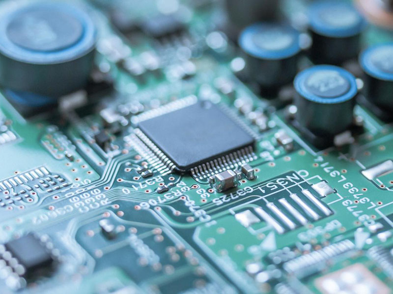
The rapid technological advancements in LED power supplies have led to significant improvements in recent years, resulting in faster product upgrades and replacements. Among the crucial stages of LED power supply development, PCB design plays a vital role. A well-executed PCB design ensures minimal electromagnetic interference and enhances the stability and safety of the entire LED switching power system. In this blog, we will explore the correct methods for PCB circuit design in LED switching power supplies, considering the placement of components, the layout of current loops, and the significance of filtering capacitors.
The Importance of PCB Design in LED Switching Power Supplies
Research and market practices have demonstrated that even if the circuit schematic is well-designed during the initial development phase, PCB design issues can adversely impact the reliability of electronic devices. Inadequate considerations for power and ground lines can lead to interference and result in degraded product performance. Therefore, adopting the right approach in designing PCBs is crucial to achieving optimal results in LED switching power supplies.
Critical Current Loops in LED Switching Power Supplies
A typical PCB for a switching power supply incorporates four current loops:
- Input signal source current loop
- Power switch AC current loop
- Output rectifier AC current loop
- Output load current loop
The input loop charges the input capacitors with nearly DC current, where the filtering capacitors act as wideband energy storage elements. Similarly, the output filtering capacitors store high-frequency energy from the output rectifier while eliminating DC energy from the output load loop. Proper wiring of the input and output filtering capacitors is essential, and the input and output current loops must connect only to the terminals of the filtering capacitors.
Setting up and connecting the input and output current loops significantly influence the level of electromagnetic interference. AC energy can radiate into the environment if the connections between the input/output loops and the power switch or rectifier are not directly linked to the capacitor terminals. The power switch AC loop and rectifier AC loop carry high-amplitude trapezoidal currents with significant harmonic components at frequencies much higher than the switching frequency. Their peak amplitudes can reach up to five times the amplitude of the continuous input/output DC currents, with a typical transition time of about 50ns. Consequently, these two loops are most prone to generating electromagnetic interference and should be laid out before other printed lines in the power supply.
Arranging Components in Input and Output Loops
Three primary components form each loop in the input and output loops of LED switching power supplies: filtering capacitors, power switches or rectifiers, and inductors or transformers. These crucial components should be placed adjacently, and their positions adjusted to minimize the length of current paths between them. The ideal design flow for building a switching power supply layout aligns with its electrical design:
- Place the transformer.
- Design the power switch current loop.
- Design the output rectifier current loop.
- Connect to the control circuit of the AC power supply.
- Design the input current source loop and input filter.
Conclusion
The proper PCB circuit design is a crucial aspect of LED switching power supplies that significantly impacts their performance and reliability. By understanding the importance of current loop layouts, filtering capacitors, and component arrangements, engineers can effectively minimize electromagnetic interference and enhance the stability and safety of LED power supplies. Implementing the best practices outlined in this blog ensures that PCB design complements the well-designed electrical system, culminating in efficient and reliable LED switching power supplies.