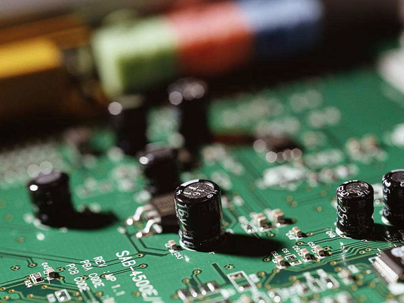
Printed circuit boards can have multiple layers depending upon the component requirements and complexity of the required device or technology. 2 layer PCB is common in simple devices. However, you have to move towards 4 layers or 6 layers of PCB for advanced levels. In this article, we will see cost estimates of 4 and 6 layer PCBs and factors that affect the cost of each setting.
4-Layer PCB Cost
The cost of making a PCB is directly proportional to the size of the board itself. The 4 Layer PCB cost practically doubles when the PCB’s length and breadth are less than 5CM. Using four layers is four times more expensive than two layers when the length and breadth are between 5-10 cm.
It is required to check with the board factory in advance whether or not it is possible to run through the hole of 0.5/0.8. If the board sub-space is restricted, it is necessary to clarify this with the board factory in advance.
The pad is the same as the welding electrodes through the hole, but not the other way around. A particular situation is another reason why the through-hole welding pad has to be at least 0.5mm bigger than the through-hole itself, owing to the manufacturing process. To begin with, stick with the more common sizes of pads.
6-Layer PCB Cost
In a six-layer PCB, the circuit board material is layered six times. So, 6 Layer PCB Cost is greater than a simple one. In this setting, two signal layers have been inserted between the planes of the four-layer PCB. Two internal planes, two internal layers, two exterior layers, one ground layer, and one power layer make up a six-layer stack.
Components having a high net count and fine pitch may be used in a 6-layer stackup to keep EMI at bay. The EMI performance of this PCB is enhanced, and the signal routing for high- and low-speed signals is expanded. Both high-speed and low-speed signals are routed via the two internal layers.
In most circumstances, PCB designers favour a 6-layer stackup over an 8-layer or 4-layer stackup. However, this isn’t always the case. Engineers and designers may use a typical 6-layer PCB to combine the requirement for inexpensive manufacturing procedures with concerns about signal integrity issues.
Our 4,6 Layer PCB

4 Layer PCB Board
Layers: 4 L Thickness: 1.6mm Out Layer Copper Thickness: 1 OZ Inner Layer Copper Thickness: 1 OZ Min Hole Size: 0.4mm Min Line Width/Space: 5mil Surface Finish: ENIG Application: Earbuds Features

6-Layer PCB Board
Layers: 6 L Thickness: 1.6mm Out Layer Copper Thickness: 1 OZ Inner Layer Copper Thickness: 1 OZ Min Hole Size: 0.4mm Min Line Width/Space: 4mil Surface Finish: ENIG Application: Monitor

6 layer PCB Board
Layers: 6 L Thickness: 1.6mm Out Layer Copper Thickness: 1 OZ Inner Layer Copper Thickness: 1 OZ Min Hole Size: 0.3mm Min Line Width/Space: 3mil Surface Finish: ENIG Application: Earbuds/p>
How to choose PCB layer and stack up?
When we make PCB stack-up design, we mainly follow below two important points:
1) Each PCB trace layer needs to have an adjacent layer as a reference (such as power or ground)
2) The adjacent ground layer and the main power layer need to keep a minimum distance to ensure sufficient coupling capacitance.
Here we will mainly introduce the explanation of the number of layers of 2-layer PCB to 8-layer PCB board:
1) stack up of single-sided PCB board and double-sided PCB board
For a 2 layer PCB board, due to the small number of layers, there is no so-called stack up problem. When we consider controlling EMI radiation, we only need to ensure the correct layout and wiring.
When make PCB design,people has been focused on the electromagnetic compatibility problem of single-layer and double-layer PCB circuit boards more and more . The main reason is that the area of the signal loop is too large, which not only produce strong electromagnetic radiation, but also produce external interference more sensitive. So if you want to reduce the problems caused by the electromagnetic compatibility of the PCB line layout, the easiest way to solve it is to reduce the loop area of the key signal.
What are the key signals?
From the perspective of electromagnetic compatibility, the key signals mainly refer to those signals that generate strong radiation and those that cause obvious interference to the outside.
Generally speaking, stronger radiation signals are periodic signals, such as low-order signals of addresses or time. And those signals that cause obvious interference to the outside are those low-level analog signals.
Therefore, single and double-layer PCB boards are often used in low-frequency analog applications less than 10KZ.
1) The power wire traces on the same layer are represented by radial traces, and the total length of the traces should be reduced as much as possible.
2) When layout the ground wire and the power wire, they are adjacent to each other. A ground wire is arranged next to the key signal wire, and this ground wire is as close as possible to the signal wire. This can reduce the loop area as much as possible and reduce the radiation signal to the outside interference.
3) If it is a double-layer PCB, we can arrange a ground wire as close as possible to the bottom of the signal wire on the other side of the PCB, and the ground wire should be as wide as possible. The resulting loop area is equal to the thickness of the circuit board multiplied by the length of the signal line.
2) Stack up of four-layer PCB boards
1. SIG-GND(PWR)-PWR (GND)-SIG;
2. GND-SIG(PWR)-SIG(PWR)-GND;
For the above two 4 layer stack up PCB designs, the main problem is that if the PCB board is a traditional 1.6mm (62mil) board thickness.Since the distance between layers will become very large, on the one hand, it is not easy to controlling impedance, inter-layer coupling and shielding, and on the other hand, it reduces the capacitance between PCB boards, which is not easy to reducing noise.
If the 4-layer PCB board stacking adopts the first design, it is often used for more chips on the PCB board. This design can achieve better SI performance, but it is not easy to control EMI electromagnetic compatibility. Usually we need to control the wiring and additional details to reduce the issue.
Notice:
The ground layer is arranged in the adjacent layer of the signal layer with the most dense signal, which is not only easy to reducing radiation, but also increases the area of the PCB board, showing the 20H rule.
If the 4-layer PCB board stack up adopts the second design, it is usually used in applications where the chip density on the PCB board is low and there is sufficient area around the chip (to place the required power supply copper layer).
The outer layers of the second 4-layer PCB design are ground layers, and the middle 2 layers are signal/power layers. The power supply on the signal layer is routed with wide wires, which can not only reduce the impedance of the current path and the signal path, but also shield the inner layer signal radiation through the outer ground layer. From the aspect of EMI electromagnetic compatibility control, it is the best 4-layer PCB structure design.
Notice:
We need to ensure that the distance between the middle two layers of signal and power mixed layers is large, and the wiring direction is mainly vertical, so as to avoid crosstalk, properly control the board area, and showing the 20H rule;
3) Stack up of six-layer PCB boards
For those designs with larger chip density and higher clock frequency, we should consider 6-layer PCB board design. The recommended stacking up is:
1.SIG-GND-SIG-PWR-GND-SIG;
This stack-up design can get a more complete signal. The signal layer is adjacent to the ground layer, and the power layer and the ground layer are paired. The impedance of each trace layer can be well controlled, and both ground layers can reduce Electromagnetic radiation better. And in the case of complete power supply and ground layer, it can provide a better return path for each signal layer.
2. GND-SIG-GND-PWR-SIG-GND;
For the design, it is only suitable for occasions where the chip density is not high. This 6-layer PCB stack-up design not only has all the advantages of the first stack-up design, but also because the ground planes of the top and bottom layers are relatively complete, it can be used as a relatively good shield to use.
Notice:
The power layer should be as close as possible to the layer that is not the main component side, because the bottom layer will be more complete. Therefore, the EMI performance is better than the first solution.
For the design of the six-layer PCB board, the distance between the power layer and the ground layer should be minimized to get good power and ground coupling.
For a PCB thickness of 62 mil, although the layer spacing is reduced, it is not easy to control the distance between the main power supply and the ground layer to be very small.
Compared with the both 6-layer PCB board design, the second cost of 6 layer PCB design is greatly increased. Therefore,we usually choose the first 6-layer PCB stack-up design.
4) Stack up of eight-layer PCB boards
For the design of 8-layer PCB board, due to poor electromagnetic absorption capacity and large power supply impedance, 8-layer PCB board is not a good stacking method.
The first of the 8-layer PCB board design:
1.Signal 1 component surface, with s little trace layer
2.Signal 2 internal wit a little routing layer, better routing layer (X direction)
3. Ground
4.Signal 3 strip line routing layer, better routing layer (Y direction)
5.Signal 4 stripline routing layer
6.Power
7. Signal 5 internal with a little routing layer
8.Signal 6 a little trace layer
2. If the reference layer is added to the 8-layer PCB design, it has better EMI performance, and the characteristic impedance of each signal layer can also be well controlled
1.Signal 1 component surface,a little wiring layer, good wiring layer
2.Ground formation, better electromagnetic wave absorption ability
3.Signal 2 strip line routing layer, good routing layer
4.Power power supply layer, which constitutes excellent electromagnetic absorption with the underlying formation
5.Ground formation
6.Signal 3 strip line routing layer, good routing layer
7.Power ground, with larger power impedance
8.Signal 4 a little routing layer, good routing layer
3. The best 8-layer PCB stacking method is as follows, because the use of multiple layers as a reference plane has very good geomagnetic absorption ability.
1.Signal 1 component surface, a little wiring layer, good wiring layer
2.Ground formation, better electromagnetic wave absorption ability
3.Signal 2 strip line routing layer, good routing layer
4.Power power supply layer, which constitutes excellent electromagnetic absorption with the underlying formation
5.Ground formation
6.Signal 3 strip line routing layer, good routing layer
7.Ground formation, better electromagnetic wave absorption ability
8.Signal 4 a little routing layer, good routing layer
For how to choose the number of PCB board layers and what kind of stacking up of PCB board, we should consider many factors such as the number of signal networks on the PCB board, device density, PIN density, signal frequency, board size, etc.
The more the number of signal networks, the greater the device density, the greater the PIN density, and the higher the signal frequency. The design should try to use a multi-layer board design. In order to get better EMI performance, it is best to ensure that each signal layer is a reference layers.
How to distinguish between 4-layer PCB and 6-layer 6 PCB?
If we want to identify the quality of PCB in the electronics industry, the first thing we think of is the number of layers of PCB Printing, Since there are single-layer board, double-layer board and multi-layer board in layer of PCB.
Among multi-layer PCB, the most common is 4-layer PCB and 6-layer PCB. What is the difference between them? Because the manufacturing cost of PCB is closely related to the number of layers of PCB, in other words, the price of 6 layer PCB is higher than that of 4 layer PCB, so how to identify the number of layers of a PCB? In this section, we will introduce two methods to guide you how to find their differences.

Check the through hole of PCB
If there is a through hole on the front in PCB,while it can not be found on the back, it is likely that the PCB is a 6-layer PCB or an 8-layer PCB instead of a 4 layer PCB. Because the 4-layer PCB needs through holes to conduct 4-layer current, the through holes will run through the whole circuit board. We can find the holes on the front and back, while there are embedded through holes in the 6-layer PCB or 8-layer PCB, so you may only find the through holes on the front and not on the back.

Check the wires at the front
Since the number of layers of 6-layer PCB is more than 4 layers, the wiring space of 6-layer PCB is larger. In other words, the wiring of 4-layer PCB is more compact, hence the wires of 4-layer PCB are more than 6 layers for each layer of PCB. we can check the wiring on the front of PCB. If the wiring is compact it is the 4-layer PCB, otherwise it is 6-layer PCB.
The above is two simple method to identify 4-layer PCB and 6-layer PCB by naked eye. If you need to explore more there are many other methods.
Factors Affecting the Cost of PCBs
The final cost of your PCB depends on the design and intended application of the board. To put it another way, if you need a simple PCB for everyday usage, the price will be far lower than if you need anything more advanced.
As a result, this is merely a general evaluation of the elements that determine PCB costs. Several real-world elements influence the cost of a printed circuit board (PCB), including 4 Layer PCB costs. A PCB’s manufacturing cost is largely influenced by its size, several layers, and material type, which have a significant effect.
So, the factors influencing the 4 layers or 6 Layer PCB Costs are the following:
- Choice of Materials
In any business, the cost of a product is directly related to the kind of production material used. When it comes to the inside of a vehicle, leather seats are more expensive than those made of fabric or cloth. As a result, it’s easy to see how the same idea might apply to PCB production. PCBs for high-intensity applications, such as those used in the petroleum or aircraft sectors, are often laminated with FR4 (flame retardant 4) material. Here are some things to keep in mind as you begin the process of selecting the right materials:
- Thermal Reliability
Determine the PCB application’s expected temperature range. Ensure the temperature rating of the material you choose falls within the allowed range. The material must not only operate within a specified temperature range but also do so in a regulated environment without overheating for an indeterminate period. Temperature reliability if you want to utilise a PCB in a high-temperature setting, be sure it passes this test.
- Temperature Tolerance
This specifies the board’s capacity to endure high temperatures without causing excessive heat to be transferred to the connected or nearby components. The term “Signal Performance” refers to a material’s ability to maintain a steady stream of electrical signals during its entire working cycle. As you may have guessed, this is essential to the proper operation of a PCB. The material’s capacity to endure the anticipated physical stresses of its applicational usage is the primary consideration in determining its mechanical properties.
- Dimensions
Unfortunately, size does matter, particularly when it comes to the expense of a product. The ultimate cost of the PCB will be influenced by the size of the board you need. When it comes to panel use, this is also true. A PCB’s total cost is influenced greatly by these two criteria.
Note: The size of your circuit board will be determined by the number of circuits you need for your specific application or design.
- Layers or Stacks
The more layers, as previously said, the more expensive it becomes. These price increases also consider the size and type of materials used by the manufacturer in its manufacturing process.
A broad comparison of the price rises is shown in the following table:
- Layers 1 and 2: (35 percent to 40 percent cost increase)
- Increasing the number of layers from two to four (35 percent to 40 percent cost increase)
- From four to six layers: (30 percent to 40 percent cost increase)
- From six to eight layers: (30 percent to 35 percent cost increase)
- From 8-Layer to 10-Layer: (20 percent to 30 percent cost increase)
- A shift from 10-layer to 12-layer construction (20 percent to 30 percent cost increase)
It adds a second layer that results in one of the largest price increases in the production process. Since this increases the number of stages in the manufacturing process, it is obvious that this is the case (lamination process).
The more layers there are, the longer the manufacturing process will take and the more resources it will use. So, 6 Layer PCB Cost and manufacturing time will be higher than lesser layers.
- Finishing
The cost of your PCB design will be affected by the finish you pick. However tiny, it is nevertheless a contributing component. You may choose one finish over another because it is of better quality or has a longer shelf life.
The following are some of the most common finish types (surface treatments):
- HASL is a good choice as a soldering material
- You can also have improved solderability with LFHASL.
- OSP provides better solderability
- Al (aluminium) wire bonding and greater solderability may be achieved using IMM Ag.
- IMM Sn provides solderability.
- Solderability, Al wire bonding capability, and a contact surface are all features of ENIG
- ENEPIG has a superior contact surface, Al wire bonding, and solderability
In terms of solderability and contact surface, Elec Au is a superior choice to Al and Au (gold) wire bonding.
- Hole Dimensions on the Board
The board’s hole size and quantity will affect the ultimate manufacturing cost. To create holes as small as possible, you’ll need specialist equipment. As previously said, the more holes you require, the more stages and manufacturing time it takes; hence, the higher the project’s cost. The board’s design is the most important component when it comes to this issue.
- Trace Width and Spacing
This includes the minimum trace width and the spacing between each trace. If you ask any engineer, they’ll tell you that having enough trace width is essential if you want to transport current on a PCB without harming or overheating it.
The first step in determining the width of a trace is to make sure that the design is correct (simulation). Trace width and current carrying capacity are inversely proportional to board size. Wider (thicker) traces will need more materials and labour, even if other reasons limit existing carrying capacity. This thing will increase the price.
In short, there is a direct association between board thickness and pricing. There is a price difference between thicker and thinner boards, but it also relies on the quality of the material. It is obtaining, laminating, and forming a PCB from thicker materials. Even if the design you are looking for is rather simple, this is particularly true.
- Specifications
Additional costs are inevitable for more complex designs or bespoke or unique requirements. Because of the additional effort, resources, and even specialised equipment required in the manufacturing process, these design requirements are more expensive to produce. However, the usage of simulation might offer a far greater grasp of your board’s cost and associated design needs before making any final design choices.
Final Words
Production costs are affected by the number of layers. Many considerations, including the complexity of the design, attention to SI concerns and more, are considered when determining the number of layers.
Generally, the 4 Layer PCB cost is greater than the 6 Layer PCB Cost,click here to know more 2 Layer Vs. 4 Layer PCB Cost. But other things like material, finishing, trace width etc., also affect the cost estimates. PCB makers and designers often work together to determine how many layers your design needs.