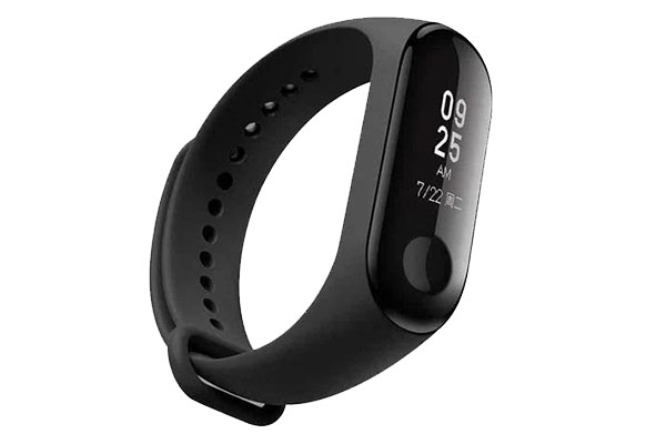
Smart bracelets have gained significant popularity in recent years, capturing the attention of consumers and influencing the electronic product market. These devices typically consist of various components, including RF circuitry, clock circuitry, memory circuitry, sensor circuitry, and a main control MCU unit. The PCB layout for smart bracelets is usually compact, often utilizing single or double-sided surface-mount technology, with 4 or 6-layer boards being common. In this post, we will explore some essential considerations for PCB design in smart bracelets to ensure optimal performance and functionality.
Partitioned Layout and Wire Routing Protection:
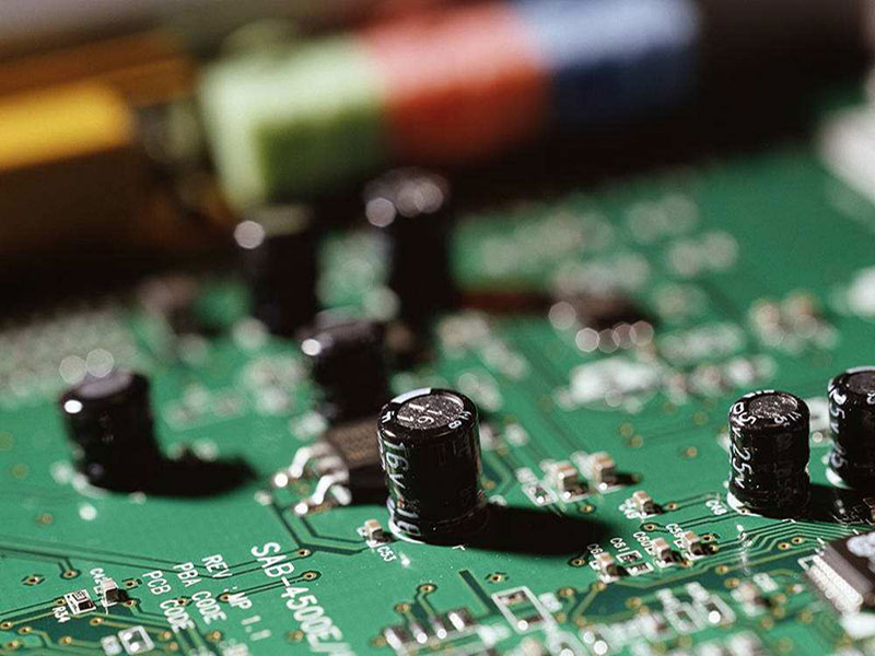
A well-organized partitioned layout is crucial in smart bracelet PCB design. As smart bracelets are essentially collections of digital circuit elements, designing circuit modules with appropriate resistor and capacitor distributions simplifies the overall design and facilitates easy troubleshooting. Additionally, when routing clock and crystal oscillator circuits, creating the shortest possible paths to their target devices is essential. Care should be taken to avoid interference from data lines, ensuring system stability.
Critical signal traces, such as those related to clock generation and crystal circuits, should be protected. This protection may involve using copper pours or ground shielding to minimize interference. Special attention must be given to the crystal oscillator section, where copper pours may need to be removed to optimize performance.
Handling RF Circuitry:
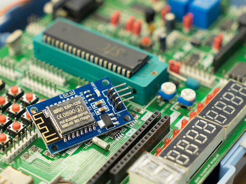
Smart bracelets often rely on wireless communication, typically utilizing Bluetooth for data transfer and synchronization with smartphones. The RF section is a crucial design part and requires careful attention. For devices solely focused on data transmission without audio capabilities, low-power Bluetooth is often the preferred choice. During the design phase, factors like the shape and layout of the Bluetooth antenna and the choice of materials for the bracelet’s casing can significantly impact overall performance. Collaboration with an experienced RF antenna engineer can be invaluable in achieving optimal results.
ESD Protection:
Electrostatic discharge (ESD) protection is vital for smart bracelets to meet the relevant product standards and regulations in different countries and regions. Incorporating ESD protection into the design and performing thorough ESD testing post-design ensures that the product can withstand electronic testing in various markets.
Provision for System Upgrades:
Facilitating convenient software upgrades is essential for smart bracelets. As these devices continually undergo development and improvement, offering the ability to upgrade software provides users and enthusiasts with a sense of satisfaction. Two common methods for software upgrades are via USB interface or wireless transmission. The decision on which method to adopt should be made during the early planning stages, considering both hardware and software considerations.
Conclusion:
Smart bracelets represent a popular and dynamic product category in the electronics market. Efficient PCB design is crucial to ensure the proper functioning and performance of these devices.
By considering the points, designers can create smart bracelets that deliver seamless connectivity, exceptional functionality, and a satisfying user experience. As this technology evolves, embracing these design considerations will remain essential to stay competitive in the smart bracelet market.