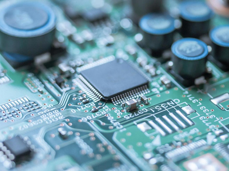
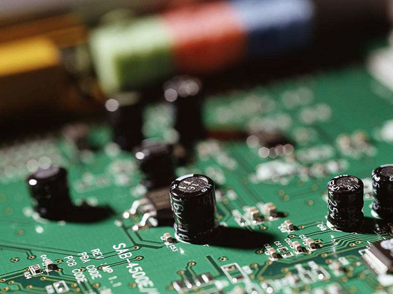
High-frequency PCB design is crucial for ensuring the proper functioning of electronic devices in various electromagnetic environments. It involves careful consideration of transmission lines, insulation materials, ground planes, and signal traces to minimize signal degradation and electromagnetic interference. In this blog, we will explore essential techniques and methods to achieve efficient high-frequency PCB design for electromagnetic compatibility (EMC).
45° Angle Traces for Reduced Return Loss
To mitigate return loss, using 45° angled traces for sharp turns in the PCB layout is essential. These angled traces help maintain signal integrity and reduce signal reflections, especially in high-frequency applications.
Controlled Dielectric Materials for Enhanced Performance
Choose high-performance PCBs with controlled dielectric constant values for each layer. This practice helps in effectively managing the electromagnetic fields between insulation materials and adjacent traces, reducing signal distortion and loss.
Precise PCB Etching Specifications
High-frequency PCBs require precise etching specifications to maintain signal accuracy. Consider specifying a line width total error of +/- 0.0007 inches, managing undercut and cross-sectional shape of traces, and specifying plating conditions for sidewalls. Properly managing trace geometries and coating surfaces is crucial to address skin effect issues related to microwave frequencies.
Minimize Lead Inductance and Opt for SMT Components
In high-frequency environments, it’s advisable to avoid using components with leads, as they introduce lead inductance. Instead, opt for surface mount technology (SMT) components, which offer better high-frequency performance and reduced parasitic effects.
Avoid Plated Through-Holes (PTH) on Sensitive Traces
Plated through-holes (PTH) on sensitive PCBs can introduce lead inductance and should be avoided. Instead, consider alternative methods such as blind vias or buried vias for connecting signal layers, which reduce electromagnetic interference.
Incorporate Abundant Ground Planes
Include multiple ground planes in the PCB design and connect them using via stitching to counter the impact of 3D electromagnetic fields on the circuit board. Adequate grounding helps in reducing noise and enhances signal integrity.
Choose Non-Electrolytic Nickel or Immersion Gold Plating
Avoid using Hot Air Solder Leveling (HASL) for plating, and instead, opt for non-electrolytic nickel or immersion gold plating. This surface finish provides a better skin effect for high-frequency currents and minimizes lead requirements, thereby reducing environmental pollution.
Employ Solder Dams for Solder Mask
To prevent solder paste flow, use solder dams (also known as solder mask dams). However, covering the entire PCB surface with solder mask can lead to variations in electromagnetic energy in microstrip designs. Carefully manage signal transitions between microstrip and coaxial cables to minimize signal loss and noise.
Electromagnetic Compatibility (EMC) Design
EMC design ensures electronic devices can function effectively and harmoniously in various electromagnetic environments. It involves suppressing external interference while also reducing the device’s electromagnetic emissions.
Optimal Trace Width Selection
To minimize the impact of transient currents and induced interference, choose trace widths that result in lower inductance. Short, precise traces are preferred as they contribute to reducing electromagnetic interference. For discrete component circuits, a trace width of approximately 1.5mm is suitable, while widths between 0.2mm and 1.0mm are commonly used for integrated circuits.
Strategic Routing
Equal-length routing can help reduce trace inductance but increases mutual inductance and distributed capacitance between traces. If possible, adopt a cross-hatch or grid-like routing pattern, where one side of the PCB contains horizontal traces and the other has vertical traces, interconnected using plated-through holes.
Minimizing Crosstalk
To mitigate crosstalk between PCB traces, avoid lengthy parallel routing of traces and ensure proper spacing between traces. Signal lines should not intersect with ground or power lines. Implementing ground traces between sensitive signal lines can effectively suppress crosstalk.
Suppressing Electromagnetic Radiation
In high-frequency PCB designs, attention should be paid to reducing electromagnetic radiation caused by signal traces. To achieve this:
Maintain trace continuity to prevent abrupt changes in trace width.
Place clock signal traces close to the ground plane return path and locate drivers adjacent to connectors.
Position bus drivers next to the buses they drive. For off-board signals, place drivers close to connectors.
Route data buses with a signal ground trace between every two signal lines. Consider placing the least critical address lines close to the ground return path, as they often carry high-frequency currents.
Arrange high-speed, medium-speed, and low-speed logic circuits according to best practices.
Controlling Reflection Interference
To suppress reflections at the termination of signal traces, strive to minimize trace lengths and use slower signal rates when possible. Termination matching can be applied when necessary by adding resistors of the same value at the end of transmission lines. Typically, termination matching is necessary for TTL circuits with higher speeds for trace lengths exceeding 10cm. The resistor value should be determined based on the output drive current and maximum sink current of the integrated circuits.
Implementing Differential Signal Pair Routing
Differential signal pairs that are routed closely together also experience mutual coupling, which can reduce EMI emissions. Since differential signals are often high-speed signals, high-speed design principles also apply to their routing. It is crucial to ensure that the characteristic impedance of the differential pairs is continuous along the entire length of the traces. In practical applications, efforts should be made to ensure that the differential pairs have identical impedance and length. Differential traces are typically routed as pairs and should maintain a constant distance between them. It is preferable to keep them as close together as possible.
Conclusion
Designing high-frequency PCBs requires careful consideration of various factors, including trace angles, dielectric materials, grounding techniques, and signal routing. Following the recommended techniques and strategies discussed in this blog will improve signal integrity, reduced electromagnetic interference, and enhanced electromagnetic compatibility. Achieving optimal high-frequency PCB design is essential to ensure the reliable and efficient performance of electronic devices in complex electromagnetic environments.When you finish designing a high-frequency PCB, you need a real manufacturer to help you realize the final work. If you are looking for some top PCB manufacturers, you can visit here.


