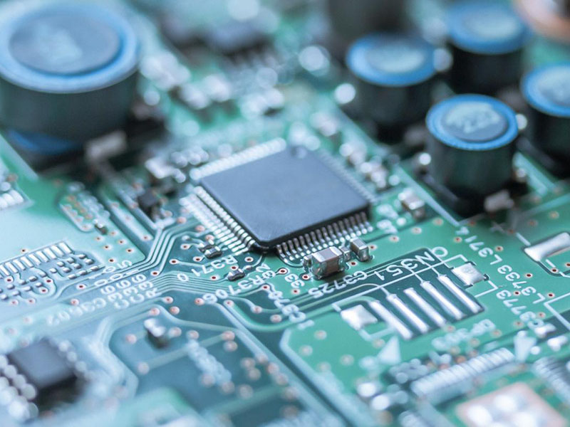
Q1: What is the cause of poor wetting during PCBA assembly?
A: Poor wetting during soldering occurs due to various reasons:
Presence of gases on the substrate surface during wave soldering.
Residual metals in solder exceeding 0.005%, reducing flux activity.
Surface contamination on soldering areas or component surfaces, such as silver sulfide or oxide on tin surfaces, leading to poor wetting.
Solution:
Adhere strictly to the corresponding soldering processes.
Ensure thorough cleaning of PCB and component surfaces.
Opt for appropriate solder and set reasonable soldering temperatures and durations.
Q2: What causes the phenomenon of “tombstoning” in components during assembly?
A: Tombstoning, where one end of a component fails to contact the solder pad and stands upright, arises from various factors:
Solder paste wetting properties.
Inherent component shapes prone to tombstoning.
Rapid or uneven heating during reflow soldering.
Incorrect solder paste selection, lack of preheating, or wrong soldering zone dimensions.
Solution:
Set appropriate solder paste printing thickness.
Establish controlled temperature ramp-ups during reflow.
Store and handle electronic components according to specifications.
Minimize surface tension on component ends during solder melt.
Preheat PCBs uniformly to ensure even heating during soldering.
Q: What methods can prevent the formation of soldering voids during PCBA assembly?
Q1: How can prolonged exposure to air be prevented for PCBs and components to avoid moisture loss?
A: Implement baking as a preventive measure. PCBs and components exposed to air for extended periods can undergo baking, effectively preventing moisture loss.
Q2: What measures should be taken regarding solder paste to prevent the occurrence of soldering voids and solder balls?
A: Several steps can be taken regarding solder paste:
Opt for high-quality solder paste to minimize issues.
Strictly adhere to the solder paste stirring process, minimize exposure time to air, and promptly reflow after printing.
Q3: How crucial is workshop humidity control in preventing soldering voids?
A: Workshop humidity control is paramount. Maintain planned monitoring of workshop humidity levels between 40-60% to prevent moisture-related issues.
Q4: How can optimal furnace temperature profiles help prevent soldering voids?
A: Setting reasonable furnace temperature profiles and performing daily temperature tests twice help optimize profiles. Avoid excessively rapid heating rates.
Q5: What considerations should be made regarding flux application to avoid soldering voids during wave soldering?
A: Ensure moderate flux application during wave soldering to prevent excessive flux and ensure proper application.
Q6: How can the optimization of reflow furnace temperature profiles contribute to minimizing soldering voids?
A: Optimize reflow furnace temperature profiles by ensuring preheat zone temperatures meet requirements without being too low, allowing sufficient flux evaporation, and avoiding excessively rapid heating rates.
Q: What are common issues encountered during PCBA board soldering, and how can they be resolved effectively?
A:
Q1: How does unstable soldering temperature affect PCBA board quality, and what solutions exist?
A: Unstable soldering temperatures directly impact solder joint quality during PCBA board assembly. Maintaining proper temperature is crucial to prevent damage to components. Solutions involve selecting appropriate soldering equipment, conducting temperature calibration, and adjusting soldering temperature and duration based on component specifications to ensure stable soldering quality.
Q2: What causes uneven soldering spacing, and how can this issue be addressed during PCBA board assembly?
A: Uneven soldering spacing often results from irregular component arrangement or inadequate board design. To resolve this issue, plan soldering layouts in advance, arrange component positions logically, and ensure soldering spacing adheres to specified requirements. Additionally, auxiliary positioning tools like soldering templates or guide pins aid in adjusting soldering positions, enhancing overall soldering quality.
Q3: How does one ensure the robustness of solder joints to enhance PCBA board reliability?
A: The strength of solder joints directly impacts PCBA board reliability. Weak joints can lead to breakage or detachment, affecting the board’s functionality. To address weak joints, choose appropriate soldering materials and methods ensuring good contact between solder and pads. Control soldering time and pressure appropriately, utilize support fixtures like soldering jigs or adhesive to enhance joint stability.
Q4: How can one safeguard temperature-sensitive components during PCBA board assembly?
A: Components in PCBA boards, especially precision ones, are highly sensitive to temperature. Incorrect temperatures or methods during soldering can damage or impair their performance. To prevent this, employ protective measures like thermal tape or heat sinks before soldering. Additionally, maintain suitable soldering temperatures and durations to avoid overheating components.
Q5: What precautions are necessary to prevent electrostatic discharge (ESD) issues during PCBA board assembly?
A: ESD can severely damage PCBA boards and their components. Implement ESD protection measures before soldering by using anti-static clothing, gloves, and footwear. Employ suitable ESD protection devices to prevent static discharge from causing harm to the boards.
Q: What are the potential issues during PCBA manufacturing, and how can they be resolved?
A:
Q1: What are the signs and causes of various soldering problems encountered in PCBA assembly?
A: Signs like cold solder joints or bursting holes can stem from insufficient copper plating or stress on the copper during soldering. Addressing this involves analyzing plated holes before and after soldering to identify stressed areas, performing incoming material inspections, and possibly changing materials to reduce stress, as suggested by the laminate board manufacturer.
Q2: How does detachment of pads and wires occur during PCBA assembly, and what measures can prevent it?
A: Detachment during soldering may result from plating solution effects, solvent erosion, or stress on copper during electroplating. It can also be due to poor soldering techniques or high temperatures. To prevent this, provide a detailed solvent and solution list to the laminate board manufacturer, analyze the electroplating process, and ensure compliance with recommended machining methods.
Q3: What leads to excessive size changes post-assembly, and how can this issue be addressed?
A: Post-assembly size changes can result from directional construction texture ignorance or localized stress within the laminate board. To mitigate this, consistently align material according to construction texture direction and, if size changes exceed tolerance, consider changing the material or seeking advice from the laminate board manufacturer on stress release methods pre-assembly.
Hope our above answers can answer your questions, if you are looking for some top PCB manufacturers you can refer here:https://www.eashub.com/top-china-pcb-manufacturers/