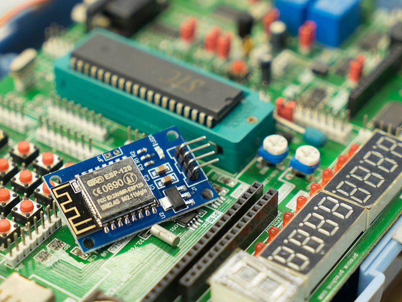
Electromagnetic Compatibility (EMC) is a crucial aspect of electronic device design, ensuring that devices can function effectively in various electromagnetic environments. The primary goal of EMC design is to suppress external interference while minimizing the device’s electromagnetic emissions, reducing its impact on other electronic devices. In this blog post, we will explore essential EMC design considerations for mobile Printed Circuit Boards (PCBs), highlighting strategies to mitigate electromagnetic interference and maintain reliable device performance.
Choosing Optimal Trace Widths:
Transient currents generate disruptive interference primarily due to the inductive components of PCB traces. To minimize this effect, reducing the trace’s inductance is essential. The inductance of a trace is directly proportional to its length and inversely proportional to its width. Therefore, shorter and wider traces are preferable for interference suppression. Signal lines like clocks and bus drivers often carry significant transient currents, necessitating shorter trace lengths. For discrete component circuits, trace widths of around 1.5mm are sufficient, while widths between 0.2mm to 1.0mm are recommended for integrated circuits.
Adopting Proper Routing Strategies:
Equal-length routing reduces trace inductance but increases mutual inductance and distributed capacitance between traces. If the layout allows, a better approach is to use a cross-hatch or grid-like routing pattern. One side of the PCB can have horizontal traces, while the other side has vertical traces, interconnected at crossover points using plated-through holes.
Avoiding Crosstalk and Interference:
To suppress crosstalk between PCB traces, it’s crucial to avoid long, parallel routing of traces whenever possible. Designers should aim to increase the spacing between traces and minimize intersections between signal, ground, and power lines. Placing a ground trace between sensitive signal lines can effectively reduce crosstalk.
Reducing Electromagnetic Emissions:
To minimize electromagnetic radiation caused by high-frequency signals traveling through PCB traces, designers should consider the following:
(a) Avoid abrupt changes in trace width or sharp trace corners. Right-angle bends should be avoided, and traces should maintain a smooth path.
(b) Clock signal traces are particularly prone to electromagnetic radiation. They should be routed close to the ground return path, and drivers should be positioned adjacent to connectors.
(c) Bus drivers should be placed close to the bus they drive, and for off-board traces, drivers should be positioned near connectors.
(d) Data bus routing should involve placing a signal ground trace between every two signal lines. Ideally, the least critical address lines should be adjacent to the ground return path, as they often carry high-frequency currents.
(e) Following a suitable layout pattern is essential When arranging high-speed, medium-speed, and low-speed logic circuits.
Suppression of Reflection Interference:
To minimize reflection interference occurring at the end of PCB traces, the trace lengths should be shortened wherever possible, and slower circuits should be used, if feasible. Terminal matching can be applied if needed, involving the addition of a matching resistor to the ground and the power source at the end of transmission lines. Typically, terminal matching should be considered for trace lengths exceeding 10cm for fast TTL circuits. The value of the matching resistor should be determined based on the integrated circuit’s output drive current and the maximum sinking current.
Employing Differential Pair Routing:
Differential signals routed close to each other can mutually couple, reducing EMI emissions. Typically, differential signals are high-speed, making high-speed design rules applicable to their routing. Ensuring consistent characteristic impedance along the entire length of the signal lines is critical for differential pair routing. The PCB traces in a differential pair should be identical, with the same impedance and routing length. Maintaining consistent spacing between differential traces throughout their length is essential, and designers should aim to keep them as close together as possible.
Conclusion:
Effective electromagnetic compatibility (EMC) design is vital for mobile PCBs to ensure optimal performance and minimize interference in various electromagnetic environments. Designers can create mobile devices that operate reliably and efficiently by carefully selecting trace widths, employing proper routing strategies, mitigating crosstalk, reducing electromagnetic emissions, and implementing differential pair routing. These practices enhance the device’s functionality and contribute to the overall reliability and performance of electronic systems in today’s interconnected world.