RF (Radio Frequency) circuit board design involves several critical factors that must be considered to ensure optimal performance and minimal electromagnetic interference. While there are guidelines to follow in RF circuit board design, practical techniques are required when facing constraints and compromises. In this blog, we will explore various aspects related to RF circuit board partitioning and delve into important considerations for successful RF circuit board design.
Types of microvias:
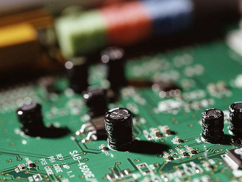
Microvias are crucial in connecting different circuit components on a PCB while maintaining minimal electromagnetic interference. They are categorized into three types: blind vias, buried vias, and through vias. Blind vias connect the top and bottom layers of the PCB to the inner layers, while buried vias stay entirely within the inner layers. Through vias span the entire PCB, enabling internal interconnections or serving as component mounting holes.
Adopting Partitioning Techniques:
In RF circuit board design, isolating high-power RF amplifiers (HPAs) from low-noise amplifiers (LNAs) is essential. This isolation ensures that high-power RF transmission circuits are kept away from low-noise receiving circuits. While this separation is relatively straightforward when the PCB has ample space, it becomes more challenging when dealing with limited space and numerous components. In such cases, placing the circuits on opposite sides of the PCB or operating them alternately instead of simultaneously can be beneficial. High-power circuits may also include RF buffers and voltage-controlled oscillators (VCOs).
The partitioning can be physical, focusing on component layout, orientation, and shielding, or electrical, dealing with power distribution, RF routing, sensitive circuitry, and grounding.
Physical Partitioning:
Proper component layout is crucial for achieving excellent RF design. The most effective technique involves placing components along the RF path and adjusting their orientation to minimize the length of the RF path. RF inputs should be far from RF outputs and as distant as possible from high-power and low-noise circuits.
An effective PCB stack-up technique is to place the primary ground on the second layer beneath the surface layer and route RF traces on the surface layer whenever possible. Minimizing the size of vias along the RF path reduces path inductance, minimizes parasitic effects, and reduces the chances of RF energy leakage to other regions of the PCB stack-up.
Careful attention must be given to minimizing interference between RF/IF signals in devices such as duplexers, mixers, and intermediate frequency amplifiers, where multiple RF/IF signals interact. RF and IF traces should ideally cross each other at right angles, with sufficient ground areas between them. Proper RF routing is critical for overall PCB performance, making component layout time-consuming in mobile phone PCB design.
In mobile phone PCBs, low-noise amplifiers are often placed on one side of the PCB, while high-power amplifiers are positioned on the other side, connected through duplexers to the RF antenna on one end and the baseband processor on the other. Special techniques, like using blind vias on both sides of the PCB, can help minimize the negative effects of vias on RF energy transmission.
Metal Shielding:
In cases where it is challenging to maintain sufficient isolation between multiple circuit blocks, metal shielding can be employed to contain RF energy within specific areas. However, metal shielding also has drawbacks, such as increased manufacturing and assembly costs.
Irregularly shaped metal shielding is challenging to produce with high precision, while rectangular or square metal shields may restrict component layout. Metal shields can impede component replacement and fault troubleshooting, and their attachment to the ground plane consumes valuable PCB space.
To ensure the integrity of metal shielding, digital signal lines entering the shield should follow inner layers, with the next layer being a ground plane. RF signal lines can exit the metal shield through small gaps at the bottom, with ample ground area surrounding the gaps. Ground connections on different signal layers can be achieved through multiple vias. Despite these drawbacks, metal shielding remains effective, often being the only viable solution to isolate critical circuits.
Power Decoupling Circuits:
Effective power decoupling is essential to minimize noise in RF chips, especially those integrating linear circuits. Typically, each chip requires up to four capacitors and one isolation inductor to filter all power supply noise.
The minimum capacitor value is determined by the capacitor’s resonance frequency and lead inductance (C4). C3 and C2 usually have relatively larger values due to their own lead inductance, resulting in less effective RF decoupling. However, they are suitable for filtering lower-frequency noise signals. RF decoupling is achieved with inductor L1, preventing RF signals from coupling into the power supply lines. Due to the potential for all traces to act as antennas, isolating RF signals from critical lines and components is crucial.
The physical positioning of these decoupling components is also critical. The layout principles for these components include placing C4 as close to the IC pin as possible and grounding it. C3 should be closest to C4, and C2 should be closest to C3. The connection between the IC pin and C4 should have the shortest trace possible. The ground terminal of these components, especially C4, should be connected to the chip’s ground pin via the first ground layer beneath the PCB surface. The vias connecting the components to the ground layer should be placed as close to the component pad as possible, and using blind vias on the pad can minimize inductance. Inductor L1 should be placed near C1.
In some cases, an integrated circuit or amplifier may have an open collector output, necessitating a pull-up inductor to provide a high-impedance RF load and a low-impedance DC power source. The same principles apply to decoupling the power end of this inductor. Some chips require multiple power supplies, necessitating two to three sets of capacitors and inductors for proper decoupling. If there is insufficient space around the chip, the effectiveness of decoupling may be compromised. Additionally, inductors should not be placed parallel to each other, as this would create a transformer with mutual inductance causing interference. Their spacing should be at least equal to the height of either inductor, or they should be arranged at right angles to minimize mutual inductance.
Conclusion:
Designing RF circuit boards involves balancing multiple factors to achieve optimal performance, minimize interference, and meet space constraints. Microvias, partitioning techniques, metal shielding, and proper power decoupling are critical aspects of successful RF circuit board design. By carefully considering these factors and implementing practical strategies, engineers can develop high-performance RF circuit boards that meet the demands of modern communication systems and devices.
Hope our above answers can answer your questions, if you are looking for some top PCB manufacturers you can visit here.