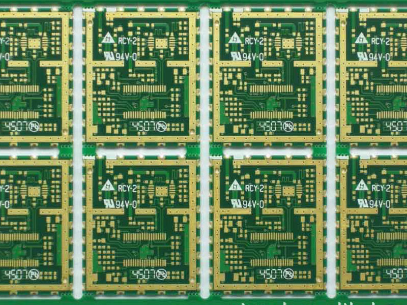
High voltage PCB operates at greater voltages than the typical rail voltage. Mains-powered power supply, Inverters, and EV chargers are examples of this type of board. High voltage does not have a predetermined threshold. A good starting point would be 100 volts for printed circuit boards—this is the normal range of voltage.
However, over 100 volts need extra considerations that you would need to be made in the design of PCB, especially for industrial use. Otherwise, your PCB can catch fire, your device can be broken, or it can result in any other accident.
- Dielectric Strength
Dielectric strength is the greatest electric field that a material can endure before losing insulating qualities. For most PCBs, FR4 would be the best choice. Your PCB material’s dielectric strength has to be checked first.
Although the FR4 material is certified for 300 millimeters per mil, IPC regulations demand 3.9 millimeters for 80V. It’s typically good to leave some wiggle areas and adhere to IPC specifications.
- Distance Creeping

When two conductive elements are located on the surface of an insulating substance, the creepage distance is the shortest distance between them. The long-term voltage supplied to the two conductors is the most important factor determining creepage distance.
Contamination on the board might occur over time. Therefore it’s a good idea to have some extra headroom. Datasheets for most components and layouts often provide recommendations for creepage distances. When it comes to High voltage PCB, this is a significant consideration.
- Distance to Clear
When two conductors are close enough to touch, this is known as clearance. The air’s dielectric strength is what determines how much clearance there is. 3KV per mm is the typical rate at which air breaks down. When moisture and contaminants are present, this number can be significantly lower. Depending on the design type, the IPC standards prescribe varying clearance distances.
Packages with a high enough pin pitch for most components are already compatible. For example, a 600V rated Mosfet will often be packaged in a TO-220 or TO-247.
- Solder Mask
Insulation is also provided via the solder mask. As a result, they’re ideal for use on circuit boards with extremely small pin pitches and high voltages across the pins. For fine-pitch PCBs, it is critical to have a manufacturer that can put a solder mask between the two PCBs.
Principles of High Voltage PCB Design
The following things must be kept in mind before designing high voltage PCBs:
- Routing
These are the most critical aspects to keep in mind while routing high voltage PCB traces:
- Keeping a gap between traces with a large voltage difference.
- Not to use sharp tunes or edges as they can have a high electric field
- In the innermost layers of the circuit board, do not run any high-voltage traces
- Polygons Planes
The polygon plane clearance on all high-voltage PCBs should be raised to a safe amount, and specific board areas should be raised as well. It’s common to see a polygon pour near a trace, sending 600V toward an edge connection on a board, but not always.
The inner planes of a multi-layer PCB should also be kept at a reasonable voltage and distance from one another to prevent short-circuiting.
- Layers within the Layer
The medium voltage can be used on all levels to create multi-layers. What matters most is how well you fill the voids between the various layers. Prepreg requires a layer separation thickness of at least.005″ to ensure the integrity of the filling medium. The dielectric value will be significantly reduced if there are any voids or pockets.
A multi-layer prepreg FR4 of the conventional kind is not suitable for medium or high voltage operations. There is a lack of uniformity in the internal structure of the material, which causes it to break down too quickly. There is a decrease in the dielectric rating due to the microvoids.

EMI Factors to Consider
High voltage PCBs are renowned because of the wide range of frequencies they may produce. For the most part, keeping the loop area short and sewing as much of the ground plane as possible is the most effective way to reduce them. A metallic sheet can also be used to insulate the high-voltage components.
- Transformers with High Frequencies
A switch-mode circuit with a transformer is nearly usually used to generate a high voltage on most high-voltage boards. You must adhere to the transformer’s core insulation level in these situations. The ground plane should preferably be split between the main and secondary sides regarding the PCB layout. There should be a substantial isolation gap with cutouts on the board between the primary and secondary sides.
- Mosfets/Transistors/Switches
Most of the time, the high voltage devices will come in the right packaging to tolerate the high voltage between pitches.
It is still smart to choose the device with the biggest pin pitch if you know the voltages would be rather high. A frequent example will be to choose a TO-247 device instead of a TO-220 if there are no space limits. Similar examples may be applied to SMD devices as well.
- Passive Components
When choosing passive components, the component size is vital as it directly depends on the voltage it can bear. So let’s assume the design has 300V between an SMD resistor. Then it would be much preferable to select a package like 1206 rather than 0402. It is sometimes necessary to place numerous such components in series to alleviate voltage stress across them
- Cutouts and Slots for Isolation
There must be cutouts or isolation holes near any high voltage component of a high voltage board. These holes and board cutouts are required by numerous safety requirements in consumer goods like chargers and power supplies.
High-humidity locations and situations where contamination is a possibility might benefit from these qualities. The mechanical layer of the board is where most of the isolation slots and cutouts will be located.
Material for Developing High Voltage PCB
The low dielectric strength of standard FR-4 makes it unsuitable for use in high voltage circuit boards. The higher dielectric strength is preferable whenever cost is not an issue. A few examples of high-voltage rated materials are as follows;
- BT Epoxy
- Polyimide
- Isola
- Finishing the Board
High voltage PCB finishing is an often-overlooked but critically vital consideration. The pads’ surface quality and any visible traces are the primary considerations. The final board should be devoid of irregularities and even over the whole surface.
Sharp points or other flaws in the high-voltage pads might create an electric field that is too strong and lead to arcing.
Basic Precautions for Designing High Voltage PCB
By adopting some precautions, you can avoid any serious outcome regarding high voltage print circuit board. Following is the crux of all the information mentioned above:
- Routing
When designing a high voltage PCB, sticking to tried-and-true routing methods is critical. When designing a circuit, it’s best to have a little space between conductors with large voltage differences. Because of the high electric field concentration, it is advisable to avoid sharp edges. Running high voltage traces in the board’s interior layers is also a big no-no.
- Layers Inside a Layer
A multi-layer PCB with medium voltage on each layer is also essential. When filling up the gaps between the layers, care must be used. PCB design requires that each layer’s separation be.005″ thick to preserve overall balance. Any holes or unnecessary gaps in high-voltage PCBs affect the dielectric value.
- Geometric Polygons
The polygon plane clearance should also be increased safely in all high voltage PCBs. A multi-layer PCB’s inner planes must be properly separated and have a high voltage. Thus, electricity can flow without interruption throughout the circuit board.
- Area
You may have heard of PCBs with high voltages releasing various electromagnetic disturbances. The disturbances can be reduced if the ground plane has a limited loop area.
High Voltage PCB Design: Why Control Creepage and Clearance Distances?
Not all PCBs need to be designed with the same spacing as high voltage PCBs. If your product is working with voltages over 30 VAC or 60 VDC, then we had better consider the PCB design spacing seriously. If you are designing a high-density PCB, especially a high-voltage circuit board, then you need to pay more attention due to high density will make the spacing more complicated.
In the design of high-voltage PCB, reasonable spacing is very important, because the voltage on the PCB components makes it easier for the adjacent conductive components to generate arcs, and once the arc occurs, it will bring serious hidden dangers to the safety of products and users. In order to reduce the generation of arc belts and the risk of coming, you need to focus on the spacing when designing high-voltage PCBs, and whether the spacing is reasonable mainly includes clearance and creepage distance.
What is a clearance distance?
Gap voltage refers to the shortest distance through the air between two adjacent conductors with the potential difference in electrical appliances, that is, the shortest distance measured along the air between two adjacent conductors or one conductor and the surface of the adjacent motor casing. If the gap between adjacent components on the PCB is too small, arcing may occur between adjacent conductive components on the PCB once the specified voltage is exceeded.
However, there is no standard distance for clearance, which varies with PCB material, voltage and environment. Among them, the influence of the environment is very large, for example, the humidity will cause the air breakdown voltage to change, which may be more prone to arcing. Dust is another factor, and dust that collects on top of the PCB can reduce the distance between conductors, producing arcing.
Arcs can endanger product and user safety, so PCB spacing is a key parameter to consider when designing high-voltage PCBs.
What is Creepage path?

Similar to clearance, creepage distance is used to measure the shortest distance along the surface of the insulating material between conductors on a PCB instead of the distance in the air. PCB material and environment also affect creepage distances, and similar to clearance distances, moisture and dust can reduce creepage distances.
When we design a high-voltage high-density PCB, it may not be easy to fully meet the creepage distance, because changing the track of PCB is not a priority to meet the creepage distance. We can usually increase the surface distance or other tricks in the design, such as between the tracks. Adding slots or vertical isolation barriers between them can effectively increase the creepage distance without changing the track layout on the PCB.
How to Determine Spacing and Materials When Designing High Voltage PCBs
Since there are many different factors in high-voltage PCB design, it is best to eliminate potential safety hazards from the source when we design high-voltage PCBs. We can refer to some standard guidelines, such as:
IPC-2221, is a general standard for PCB design clearance and creepage distance guidance.
IEC-60950-1. The IEC version is the standard for any IT product that has AC mains or battery power.
FAQs
When it comes to PCBs, what constitutes high voltage?
Unofficially, a PCB with 100V or over is considered high voltage, although there is no established number.
What is the maximum voltage that a PCB can withstand?
The material does not matter as much when designing and manufacturing a low voltage printed circuit, as all printed circuit materials can withstand up to 1000 Volts.
PCB vias can carry how much current?
Using a 0.35-mm drill, you may securely transfer 2 amps of electricity. Filling them with solder can also lessen their resistance.
How hot can the PCB traces get?
To protect the PCB from discoloring and weakening over time, it is a more common practice to allow for a temperature range of 20-30°C. UL certifications might be difficult if the inside temperature exceeds 105 degrees Celsius.
Conclusion
The planning and manufacture of a high voltage PCB necessitate a high degree of accuracy. You can simply acquire a long-lasting board if you follow all of the regulations and basic practices for high-pressure guidelines.
Moreover, choosing a reliable PCB manufacturer is very important in the case of high voltage devices. Hence, the chances of accidents increase a lot with poor quality design or material.